
EPMA (Electron Probe Microanalysis) Testing Technique
The electron microprobe is an electron microbeam instrument similar to an SEM, but different in that it is highly specialized to provide superior accuracy in elemental analysis using the X-ray emissions induced by an electron beam.
Our microprobe utilizes seven wavelength dispersive spectrometers (WDS) for determining chemical information on a micron by micron scale. Each WDS can be tuned to a specific element to provide fully quantitative analysis on metallographically prepared specimens.
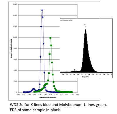
The X-ray resolution provided by the microprobe using WDS is about an order of magnitude better than EDS, which eliminates many of the pathological spectrum peak overlaps observed using EDS. In addition, detection limits are about 100 times better than EDS and elements as light as Boron can be quantitatively measured.
Microprobe Features
A few of the notable features of our system are:
- It is one of the world's fastest electron microprobes, with seven wavelength dispersive X-ray spectrometers (WDS) and a silicon drift detector energy dispersive X-ray spectrometer (SDD-EDS).
- It has the highest take-off angle of any commercial electron microprobe for the greatest accuracy and sensitivity.
- It produces ultra-fast color X-ray element maps capable of incorporating signals from both EDS and WDS detectors.
- It has the capability to discern nearly the entire periodic table of elements, from boron to uranium on a microscopic scale.
Microprobe Experience
Our microprobe analysis has been used to support research, development, manufacturing, maintenance, and repair across several industries.
Examples of the types of analyses we've conducted include:
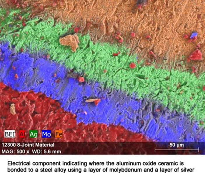
- Elemental diffusion profiles across weld and braze joints. Also across glass defects.
- Phase characterizations to identify stoichiometry of various carbides, borides, and intermetallics.
- Corrosion product identification
- Identification of residue left by foreign and domestic object damage in support of failure analyses.
- Material identification of unknown contaminants.
- X-Ray Element mapping to identify spatial variation in chemistry.
Example analysis
EPMA - At a Glance
- Information: Fully Quantitative Elemental Weight Percent with Micron Spatial Resolution, Secondary & backscattered electron images, "How Much of What is Where"
- Sample Size: Up to 51mm cube
- Detection Limits: 100 - 0.01 wt.% potentially as low as 10ppm in certain situations
- Elements Detected: Boron (B) and heavier
- Area Analysed: From 1µm x 1µm to 560µm x 500µm
- Sampling Depth: ~0.5µm - 3µm
- Image Resolution: ~200nm
- Data Output: Tables or Plots of Elemental Weight Percent, Electron Images, EDS and/or WDS spectra and X-Ray Element Maps